The semiconductor industry’s packaging technology is approaching a transition that could prove as consequential for chip performance as the move from planar to FinFET transistors a decade ago. Hybrid bonding, a technique that directly connects copper surfaces between semiconductor dies without the solder bumps used in conventional thermal compression bonding, promises finer-pitch interconnections, lower electrical resistance, superior thermal conductivity, and the ability to stack more layers in less vertical space. Samsung has demonstrated that hybrid bonding for 12 and 16-layer HBM stacks reduces thermal resistance by 20% and lowers base die temperature by more than 11 degrees Celsius. SK Hynix is conducting process verification between April and May 2026. TSMC is integrating hybrid bonding into its next-generation CoWoS packaging platform. The race to production-ready hybrid bonding is the next front in the Asian semiconductor technology competition.
The technical mechanism involves polishing copper pads on each die to atomic-level flatness and pressing them together at elevated temperature, causing the copper surfaces to bond through metal interdiffusion. The resulting connections can be spaced at pitches below 10 micrometers, quadrupling the interconnect density compared to the 40-micrometer minimum pitch of solder-based approaches. More interconnections per unit area means more data pathways between stacked dies, enabling wider memory interfaces and higher aggregate bandwidth. It means better power delivery, because the resistance of each connection is lower and more connections share the current load. And it means thinner packages, because the absence of solder bumps reduces the gap between dies, allowing more layers to be stacked within the same vertical envelope.
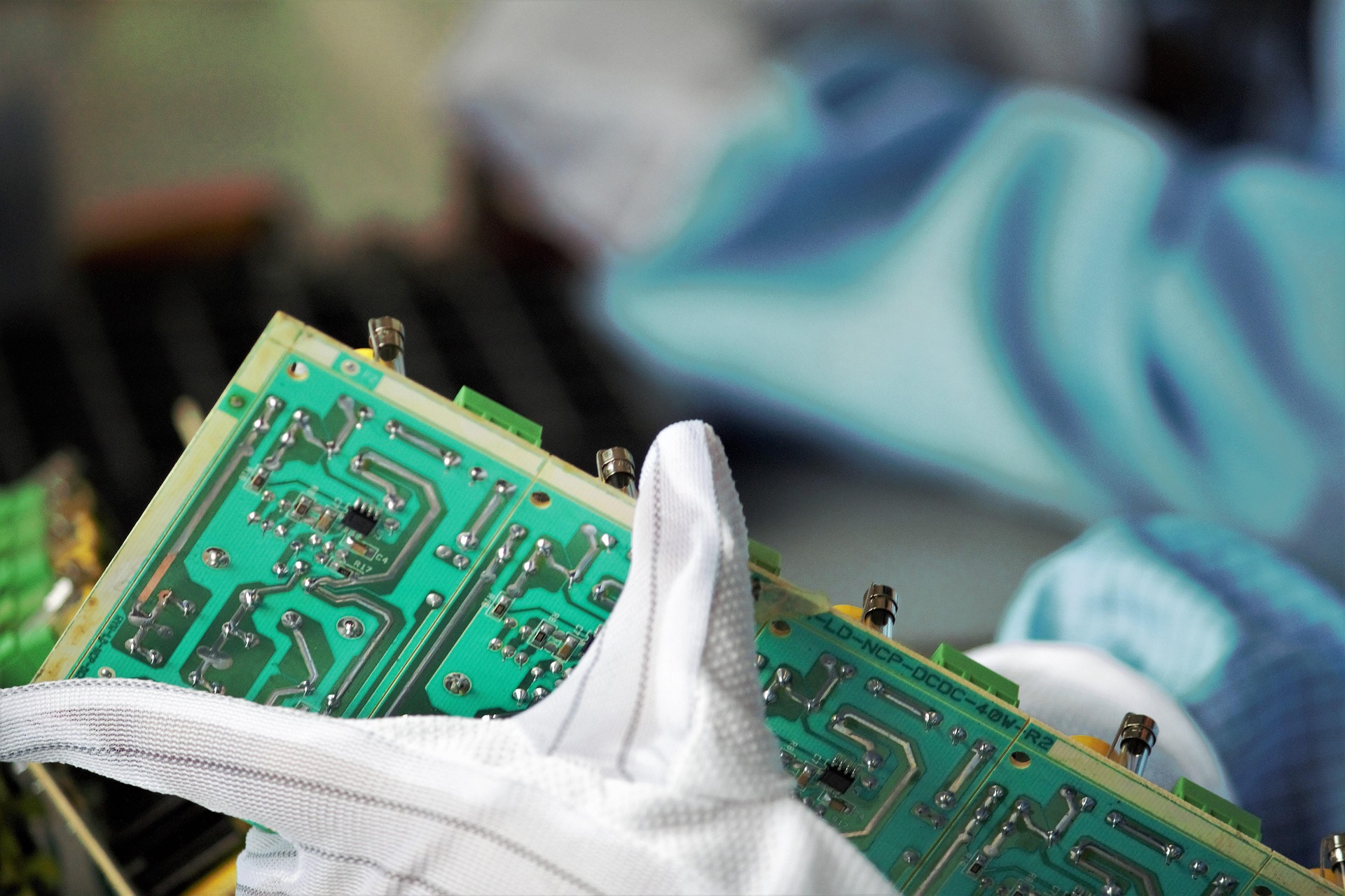
The manufacturing challenges explain why hybrid bonding has not yet replaced thermal compression bonding in volume production. The surface preparation requirements are extreme: the copper pads must be planarized to sub-nanometer roughness, and any contamination, including particles as small as a few nanometers, can cause bond failures. The alignment precision between dies must be maintained to within one micrometer across the full die area. Besi, the Dutch equipment manufacturer that dominates the hybrid bonding tool market, has reported order backlogs extending 12-18 months as chipmakers compete for the limited supply of production-capable systems.
Samsung’s position reflects its broader vertical integration strategy. The company has invested in hybrid bonding R&D across both its memory and foundry divisions, creating internal synergies where process improvements developed for HBM packaging can be applied to logic chip stacking and vice versa. The decision on whether to deploy hybrid bonding for HBM4 production or to reserve it for HBM4E variants will be clarified in early Q2 2026, according to VESI CEO Richard Blickman.
For investors in the semiconductor equipment and packaging supply chain, hybrid bonding represents a technology inflection that will redirect capital spending toward new tool categories and material requirements. Besi’s systems, priced at several million dollars each, represent a high-margin product category with limited competition. Surface preparation equipment from Disco and Tokyo Electron will see demand increases. Advanced substrate manufacturers including Ibiden and Unimicron will need to develop substrates compatible with the finer-pitch connections that hybrid bonding enables. The technology transition creates a distinct investment cycle within the broader packaging buildout, rewarding companies that have positioned their product portfolios for copper-to-copper direct bonding at scale.